Solar-Tectic receives patent for novel III-V tandem cell

Patent covers high efficiency and cost effective solar cells made on glass or flexible plastic substrates
Solar-Tectic LLC has patented a method of making III-V thin-film tandem solar cells with high performance. The patent, US 15/205,316 titled 'Method of Growing III-V Semiconductor Films for Tandem Solar Cells' is for high efficiency and cost effective solar cells made on glass or flexible plastic substrates for various industrial applications, such as rooftops to help charge battery-powered electric automobiles (EVs). The technology also looks promising for making LEDs.
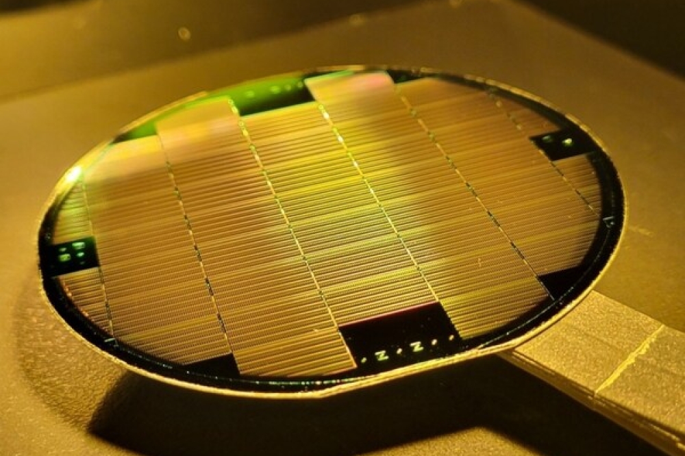
The patent (the first ever for a thin III-V layer on crystalline silicon thin-film) covers group III-V elements such as GaAs, and InGaP, for the top layer, as well as all inorganic materials, including, silicon, germanium, etc., for the bottom layer.
In the breakthrough technology here, ultra-thin films of III-V materials and silicon (or germanium) replace expensive, thicker wafers thereby lowering the costs dramatically. The inventor is Ashok Chaudhari, CEO of Solar-Tectic LLC.
III-V tandem (or multi-junction) cells built on wafers such as silicon are currently being developed in labs, with high efficiencies of around ~30 percent. The highest dual-junction cell efficiency (32.8 percent) came from a tandem cell that stacked a layer of GaAs atop crystalline silicon. Manufacturing costs are expensive especially if a germanium wafer is used as the bottom material in the two layer tandem structure.
In order to compete with low cost silicon wafer technology which is 90 percent of the solar panel market, efficiencies must not only be as high as silicon wafers or greater (21.7 percent and 26.7 percent are lab records for poly- and monocrystalline silicon wafer cells, respectively), but manufacturing costs must also be lower.
Solar-Tectic says this is achievable with its patented technology, which uses common industrial manufacturing processes and at low temperature. There is no wafer involved which saves material and energy; instead a thin film allows for precise control of growth parameters.
A glass substrate instead of wafer also allows for a bifacial cell design for increased efficiency.
A cost effective ~30 percent efficient III-V tandem solar cell in today's market could dramatically reducing the balance of system (BoS) costs, and thereby reduce the need for fossil fuel generated electricity. Silicon wafer technology based on polycrystalline or monocrystalline silicon could become obsolete.
Importantly, the entire patented process for the Solar-Tectic LLC III-V tandem cell can be environmentally friendly since non-toxic metals can be used to deposit the crystalline thin-film materials for both the bottom layer in the tandem configuration as well as in the top, III-V, layer.
The company says that the technology also has great promise for LED manufacturing using for example GaN.
A 'Tandem Series' of solar cell technologies has been launched by Solar-Tectic LLC, which includes a variety of different semiconductor photovoltaic materials for the top layer on silicon and/or germanium bottom layers. Recently patents for a tin perovskite and germanium perovskite thin-film tandem solar cell were also granted.
The ITC ruling on September 22 means that it is likely that tariffs will be imposed on crystalline silicon wafers sold in the US. These tariffs will not apply to thin-film solar cell technology, such as ST's.