KLA: Expanding within the CS cluster

Equipped with a demonstration lab capable of accommodating more than 100 process modules, KLA’s new, purpose-built facility should spur further growth of its deposition and etch tool businesses.
BY RICHARD STEVENSON, EDITOR, CS MAGAZINE
Right now, the South Wales compound semiconductor cluster is thriving. Behind those positive vibes is Vishay’s investment of SiC manufacturing technology at its Newport fab, the completion of the Centre for Integrative Semiconductor Materials at Swansea University, and most recently, the opening of a tremendous new facility for the development and production of KLA Corporation’s deposition and etch equipment.
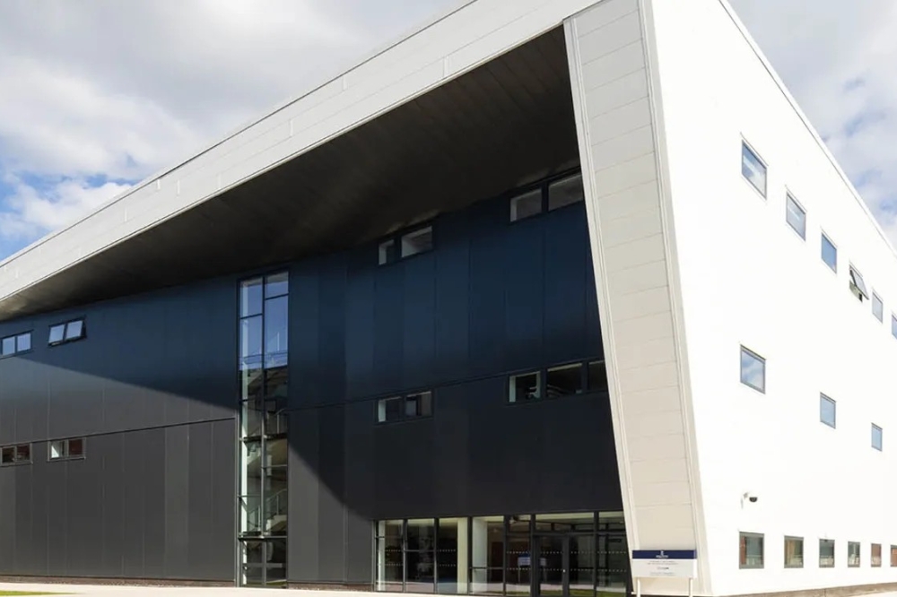
Opening on 22 May to much fanfare, KLA’s £138 million facility sits at the heart of the cluster, in an industrial area on the outskirts of Newport that’s also home to IQE and the CS Catapult.
To mark this key day in KLA’s history, the company took the opportunity to show 100 or so VIPs around its purpose-built 237,000 ft2 three-story facility. Accommodating up to 750 employees, this brand-new building features: more than 25,000 ft2 of cleanroom space for R&D; more than 35,000 ft2 for bespoke manufacturing; plenty of office space, with lots of natural light; and a canteen and a gym for all its staff.
During the opening ceremony, KLA’s VP Product Marketing, SPTS Products, Dave Thomas, spoke exclusively to Compound Semiconductor, detailing plenty of sound reasoning behind the relocation, the trends that the company is seeing within the compound semiconductor industry, and how the new facility and the management at KLA will help to continue a ramp in sales of the company’s etch and deposition tools.

In the basement of KLA’s new facility is a ‘sub-fab’, providing the necessary infrastructure for supporting tool assembly and the running of tools to aid and attract customers. Credit: Matt Lincoln
Local firm, global brand
The roots of the etch and deposition division of KLA can be traced back to the days of ElectroTech, which in 1984 established a subsidiary, Special Research Systems, in Bristol – just the other side of the Severn estuary from the CS cluster. Over the years, this company re-located to South Wales, with a couple of local moves supporting expansion of the business.
In the last fifteen years this venture has thrived, with sales of the SPTS etch and deposition tools rocketing from around $50 million to $500 million. Supporting this phenomenal growth is the acquisition by KLA in 2019, which has driven a doubling of revenue from this division and a commensurate increase in headcount. This expansion has driven demand for a bigger facility, with space not only for the expanded workforce, but also for aiding the development and demonstration of tools and processes.
Thomas believes that the acquisition by KLA came at just the right time for SPTS. “When you're going from a few hundred million towards a billion, you have to start thinking differently. You need to act more corporately, have much better control over your internal processes, and certainly be better connected with your customer base at multiple levels.”
As well as offering all this, incorporating SPTS into the KLA fold has provided the finance and bold vision for building a purpose-built facility. Without doubt, this would be located in the compound semiconductor cluster, highly valued for a number of reasons.
According to Thomas, one crucial benefit of remaining within the cluster is that it enhances joint development with local companies and universities.
“There are programmes that we have running with Swansea University, where they're helping us to understand the link between the device and the wafer process,” remarked Thomas. “Just recently, we're developing an endpoint system for silicon carbide trench etching, and we're trying to figure out how tolerant is the device to the trench characteristics.”
Thomas argues that another benefit of operating within the cluster is that is helps with discussions with local and national government, because those officials have now grasped a basic understand of the importance of the compound semiconductor industry.
From MEMS to the compounds
Sales of equipment to the MEMS industry provided initial success in the etch and deposition tool market. “We were the first licensees of the Bosch process,” explained Thomas, adding that back in 1995, they worked with this German powerhouse to develop the deep-silicon-etching Bosch process.
Today, the MEMS sector is still valued by KLA, accounting for around 10-15 percent of sales of its etch and deposition tools. However, greater revenue is coming from the compound semiconductor industry.
Here, involvement dates back several decades, with success underpinned by efforts to understand the specific characteristics of all the main materials.
Expansion into the compound semiconductor sector began with GaAs, which has some key differences to silicon from a processing perspective.
However, while it is more difficult to etch GaAs than silicon, it’s still easier than InP, according to Thomas: “You've got a very heavy metal, indium, with a very light element, phosphorus. When you come to etch it, it's very easy to etch one in preference to the other, and create a rough surface. You need to move to high-temperature etching to liberate both materials.”
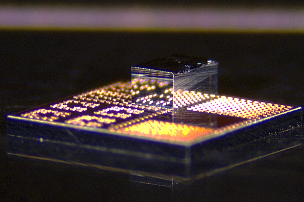
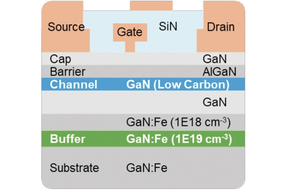
KLA also has capabilities in wide bandgap materials, particularly SiC and GaN. “Silicon carbide is very difficult to etch because it's so tough. You have to really hit it hard,” said Thomas, who explained that a markedly different approach is required for GaN, which is easily damaged. “These subtleties, they're part of our DNA now, and we understand them.”
Armed with all this hard-won expertise, KLA’s deposition and etch tools are winning sales in all the major compound semiconductor markets.
In the RF market, KLA’s process equipment is employed for the production of various devices, including those based on GaAs, InP and GaN on both silicon and SiC.
“The RF market is in a state of recovery,” said Thomas, who is expecting growth to continue over the next few years.
In the power semiconductor sector, there has been huge growth over the last few years, driven by SiC devices for electric vehicles and infrastructure. However, recently, there has been some ‘softening’, according to Thomas, who remarked that the company is also active in the GaN market. “We work with pretty much all customers you can think of in the GaN power space and the SiC space.”
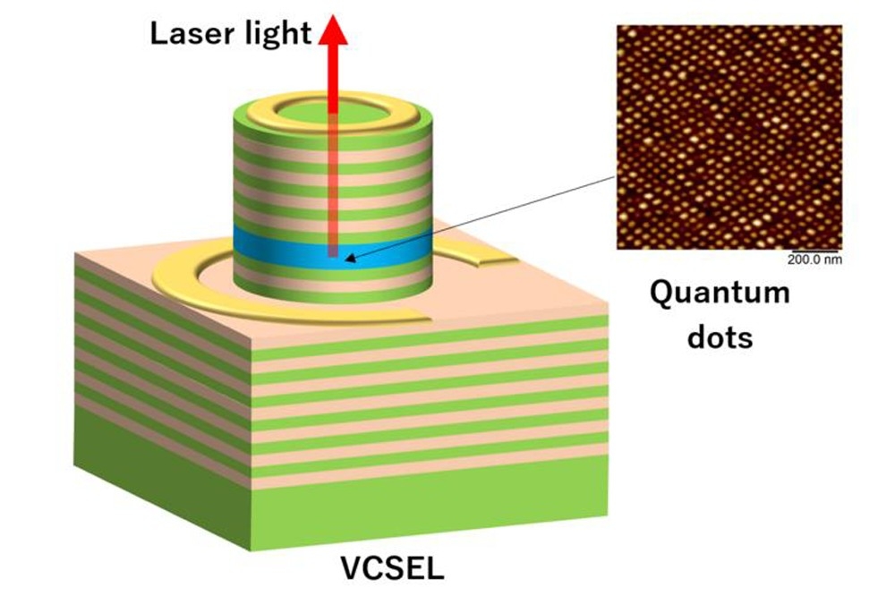
Another key sector is photonics. “This is the exciting one for me right now,” revealed Thomas, who explained that makers of lasers for optical communication are enjoying tremendous growth, and there’s also the promise of co-packaged optics.
For those in the silicon industry, advanced packaging is synonymous with flip-chip bumping. Technologies like TSMC's CoWoS that unites memory with logic have become well-established.
“The next step in that progression is to bring photonics onto that package,” argued Thomas, who elaborated by explaining that progress hinges on the addition of InP or GaAs lasers onto the silicon-centric packages.
“It's such a clash of cultures, because you've got four and six-inch wafers versus twelve-inch wafers,” remarked Thomas.
Along with his colleagues, Thomas is trying to bring the two camps together, drawing on KLA’s strong relationships between both the makers of VCSELs and edge-emitting lasers, and the big five in silicon that employ hybrid bonding. “The marriage of the two is not going to be easy, but we're right in the middle of that and we can help.”

KLA’s new facility is a very attractive place to work, with a spacious demonstration lounge (pictured), as well as a spacious foyer, a well-equipped gym, a canteen and a coffee bar. Credit: Matt Lincoln
The demo lab
One of the assets of KLA that should help in this endeavour is its new demonstration lab, able to house over 100 process modules. In this cleanroom, the company can showcase the capability of its tools and processes to its customers.
“We don't really often sell anything without demonstration first,” revealed Thomas, who explained that to win orders, it’s imperative to either prove that KLA’s tools are superior to the incumbents, when they are applied to a potential customer’s established production processes; or are capable of being employed for a new manufacturing process.
In both cases, customers tend to send wafers to KLA, which runs them through its tools and reports the data.
“We collaborate a lot during that process,” said Thomas, revealing that this can involve plenty of calls, and trips to the customer’s offices. “Better still, they come here and they sit with us in those demo rooms – and they watch, they learn, they advise, and we work together.” Typically, in this preferred modus operandi, engineers from the chipmaker will spend a week at KLA.
As well as demonstrating processes to customers, the demo room is used for R&D – this accounts for about 40 percent of activity. Efforts on this front include refining processes to make them more manufacturable, and the development of new hardware.
Managing the move
Today there are only a handful of tools in the demo lab, and the office space in the new facility is populated very lightly. Over the next six-to-nine months, groups will be making the move from one side of Newport to the other to set-up in the new facility. As this involves decommissioning and recommissioning, while meeting customer needs, it will be both an exciting and challenging time. However, there’s no doubt that these efforts will be rewarded.
“We will have a really engaged workforce and a really engaged set of customers who want to come here and work with us,” commented Thomas, who expects that the new facility will also act as a magnet to recruiting highly capable employees.
“When I have a vacancy for a product manager, I'd like to see 10 CVs from Swansea and Cardiff universities, and local schools. I want to take local talent because, to me, if we can continue to build locally from here, I think that's a really good story for us.”
Main image: On a gloriously sunny 22 May 2025, KLA welcomed around 100 VIPs to the opening of its purpose-built facility. After speeches from the company CEO Rick Wallace and the local MP, Ruth Jones – delivered in a marquee – visitors were treated to a tour around the three-story facility. Credit: Matt Lincoln