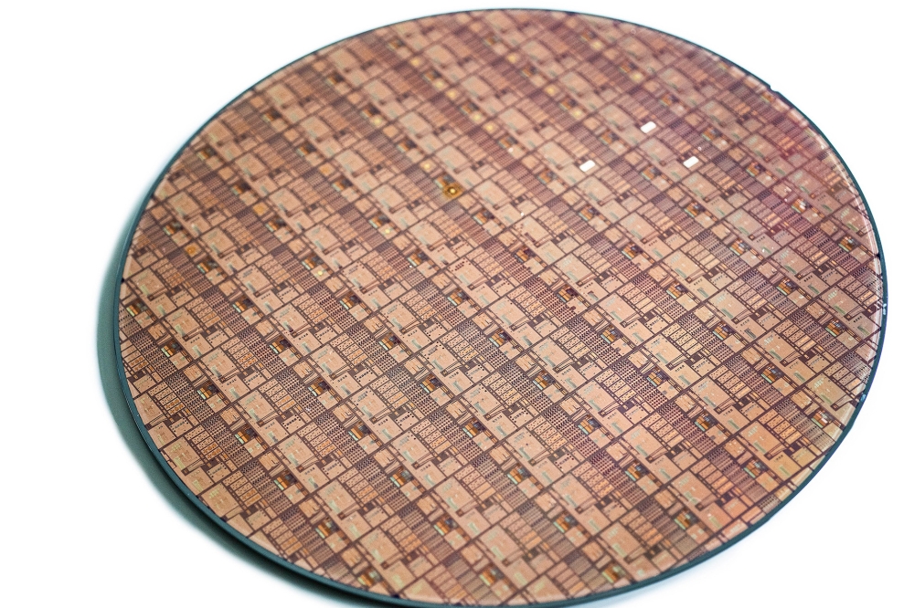
Fraunhofer team makes InP-on-GaAs wafers up to 150 mm

Working with the company III/V-Reclaim, scientists at the Fraunhofer Institute for Solar Energy Systems ISE have succeeded in producing high-quality InP on InP-on-GaAs wafers with up to 150 mm diameter.
These new wafers can effectively replace classic InP in a variety of applications, offering a scalable pathway to lower cost. The research team developed a process to deposit a thin layer of high-quality InP on GaAs. Following a special surface treatment, these wafers are delivered epi-ready, enabling customers to directly grow III-V epitaxial structures and manufacture high-performance InP-based semiconductor devices.
“Companies can use our new InP-on-GaAs substrates to manufacture high-efficiency devices”, explains Carmine Pellegrino, project manager at Fraunhofer ISE. ”However, it costs much less than InP and there are no limitations in terms of scalability to even 8-inch diameter wafers.”
The application of InP on GaAs is challenging because defects occur during the growth of the InP, which can degrade the performance of the final device. The scientists were able to avoid this by incorporating a series of 'metamorphic buffer layers' and by subjecting the fully grown InP-on-GaAs wafer to a special chemical-mechanical polishing step. After this, the wafers are shiny with very low surface roughness and defect densities below 5 x106 cm-2.
The researchers tested the material quality and performance of the new InP-on-GaAs wafers and compared them to standard InP substrates. “The results are extremely promising,” says Frank Dimroth, head of the III-V photovoltaics department at Fraunhofer ISE. “Photovoltaic cells fabricated on our engineered wafers achieve open-circuit voltages comparable to reference devices on prime InP wafers. The performance is consistently uniform across the entire 6-inch wafer, enabling reliable, high-yield production”.
As part of a series of experiments, the research team have so far produced InP-on-GaAs wafers with a diameter of 4 and 6 inches, with no obstacles foreseen for a future transition to 8-inch. Classic InP substrates, on the other hand, are currently available in sizes from 2 to 4 inches, with a 6-inch version only recently becoming available. This is because GaAs substrates are more robust and formats with a diameter of up to 8 inches are already well established in the semiconductor industry. The higher stability of GaAs also makes it possible to produce thinner wafers, which means that less material is used, and additional costs can be saved.
“Our technology naturally benefits from having GaAs as a basis,” adds Pellegrino. ”The production costs of the new substrates are significantly lower than those of InP wafers, with a savings potential up to 80 percent in mass production according to our first calculations. In addition, our approach bypasses constraints on the supply of InP.”