Increasing the power-added efficiency of GaN-based HEMTs
Engineers from Fujitsu are claiming to have broken the record for the power-added efficiency of transistors operating in the industrial, scientific and medical band.
The team’s AlGaN/GaN HEMTs produce a power-added efficiency of just over 85 percent at 2.45 GHz, beating the previous record, also held by Fujitsu, of 82.8 percent.
According to the team, the increase in efficiency results from improved crystal quality of the GaN channel and mitigation of effects of residual silicon at the interface between the substrate and the epitaxial layers.
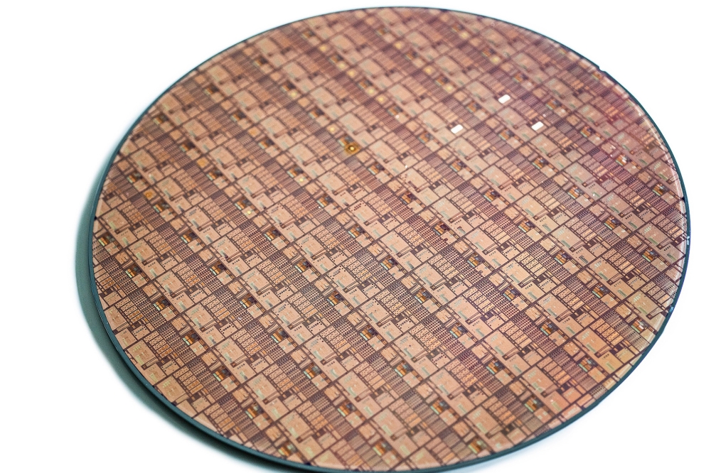
For both generations of record-breaking HEMTs, Fujitsu’s engineers have grown epilayers on native substrates – and for the latest devices, this has involved a 4-inch foundation.
Spokesmen for the team, Toshihiro Ohki, told Compound Semiconductor that while one of the benefits of using 4-inch GaN substrates is the demonstration of mass-production capability, the primary reason is that it allows the fabrication of higher-quality devices.
Fabrication of Fujitsu’s latest generation of GaN HEMTs began by repeating the first step of the process used for making their forefathers, which involved chemical pre-treatment with HF acid to remove residual silicon from the surface of the GaN substrate.
This treatment, now applied to a semi-insulating 4-inch substrate with a dislocation density of less than 5 x 106 cm-2, slashed the residual silicon concentration by two orders of magnitude, as well as the leakage current flowing laterally along the substrate surface.
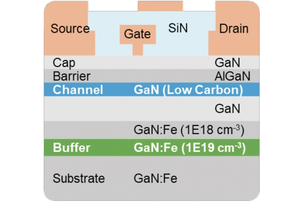
After chemical treatment, the team loaded their substate into an MOCVD chamber and deposited an iron-doped GaN buffer layer with a dopant concentration of 1 x 1019 cm-3.
“The iron-doped buffer itself is not new,” remarked Ohki, who added: “This time, we added iron at a concentration exceeding the residual silicon in GaN-on-GaN to suppress leakage current.”
To understand the effectiveness of the new buffer, Ohki and co-workers compared two samples through the use of an isolation evaluation pattern, produced by inactivating a two-dimensional electron gas (2DEG) with argon-ion implantation.
Compared with the buffer-free sample, that with the iron-doped buffer provided notably superior suppression of the leakage current.
During the growth of the epistructure, the engineers increased the III-V ratio in the GaN channel from 1600 to 8200 to reduce residual carbon and improve crystal quality.
Photoluminescence spectra, featuring a peak at around 560 nm associated with carbon-related defects, confirmed the reduction in residual carbon concentration.
To reduce the contact resistance of the ohmic electrode, Ohki and co-workers applied stripe-shaped periodic recess etching. According to the engineers, this structure ensures a more stable, lower contact resistance than a planar-type recessed structure, due to direct contact between the 2DEG and the electrodes, and the absence of a thin barrier layer. What’s more, the stripe-shaped recess structure reduces the thermal budget, which can be an origin of electron traps.
Featuring a stripe-shaped recess that reduces contact resistance from 0.38 W mm to 0.25 W mm, the team’s HEMTs, with a 0.5 mm gate length, produce a maximum drain current of 853 mA mm-1 and have an on-resistance of 4.74 W mm.
Operating at a drain voltage of 10 V, these devices produce a maximum transconductance of 288 mS mm-1 and have a threshold voltage of -1.77 V.
After setting fundamental and harmonic impedance to power-added-efficiency matching conditions, Ohki and co-workers determined that their HEMTs simultaneously exhibit a power-added-efficiency of 85.2 percent, a drain efficiency of 89.0 percent, and an output power of 44.04 dBm, which corresponds to a power density of 7.9 Wmm-1.
With a drain efficiency approaching 90 percent, Ohki and co-workers believe they are nearing the limit for this frequency.
Ohki added: “We intend to expand this technology to higher frequencies, such as millimeter waves.”
Reference
T. Ohki et al. Appl. Phys. Express 18 034004 (2025)
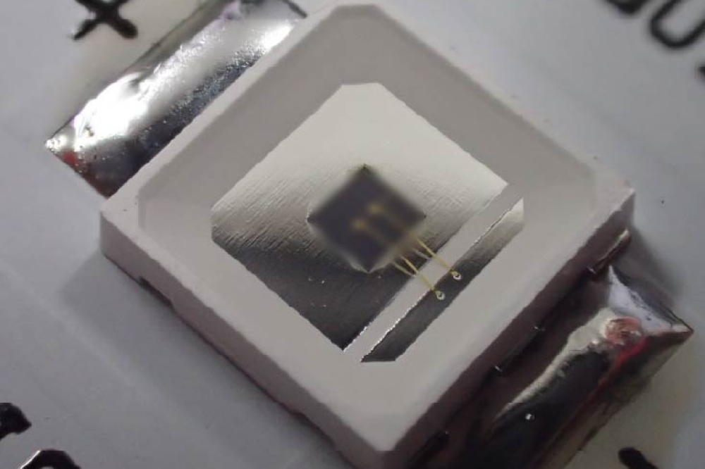
Pictured above: increasing the concentration of iron in the buffer layer helped to increase the power-added efficiency of Fujitsu’s HEMTs.