NICT-Sony collaboration makes laser breakthrough
Japan's National Institute of Information and Communications Technology (NICT) in collaboration with Sony Semiconductor has developed what is claims is the world's first practical surface-emitting laser for 1550nm comms that employs quantum dots (QD) as the optical gain medium.
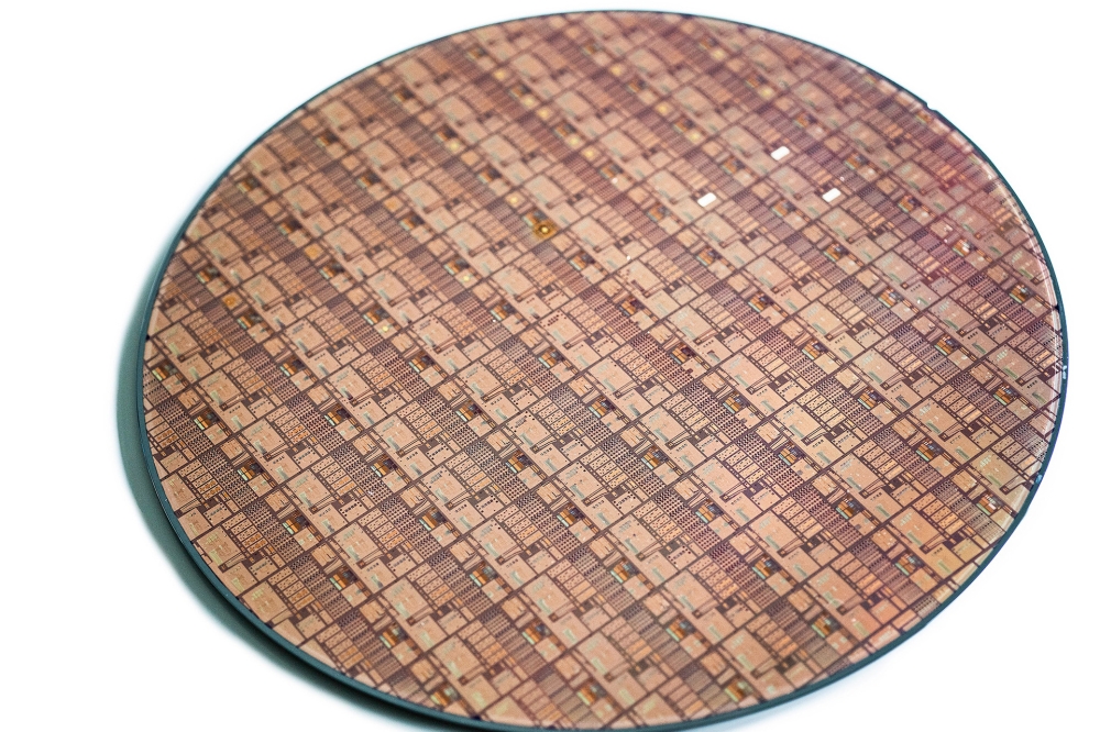
The results of this research 'Electrically pumped laser oscillation of C-band InAs quantum dot vertical-cavity surface-emitting lasers on InP(311)B substrate' were published in Optics Express, in March year.
This innovation not only facilitates the miniaturisation and reduced power consumption of light sources in optical fibre communications systems but also offers potential cost reductions through mass production and enhanced output via integration, according to the researchers.
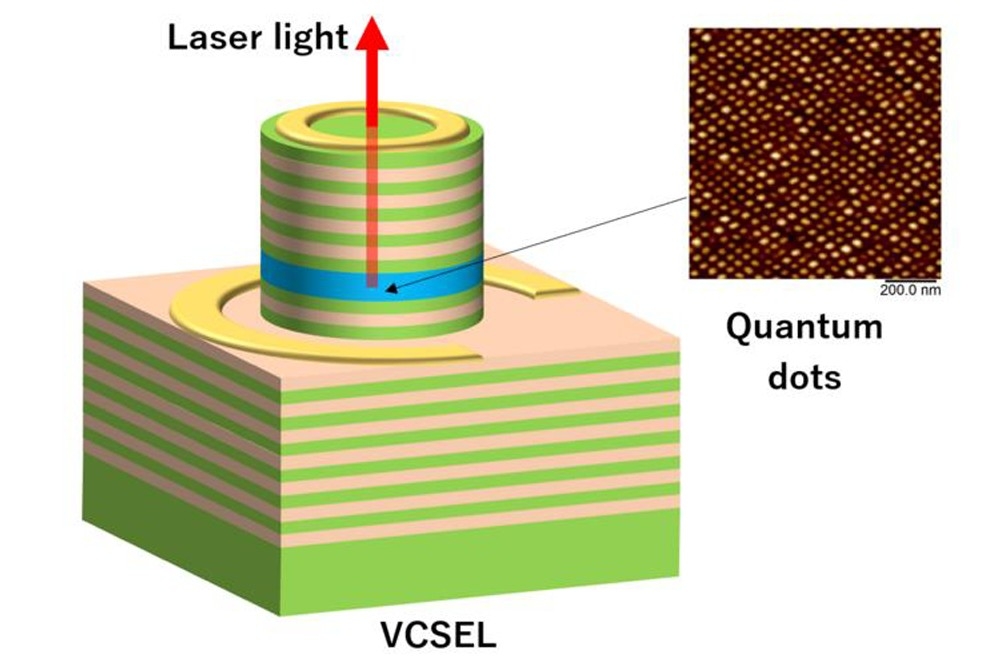
NICT's role was to develop the reflective semiconductor multilayer fabrication and quantum dot crystal growth technology using MBE. Sony undertook the device design for the entire VCSEL structure and device process technology.
Sony contributed: a device design and fabrication process that enables highly efficient current injection employing a tunnel junction. VCSELs emit light perpendicular to the wafer surface; therefore, even if quantum dots emit light, conventional electrode placement obstructs light extraction. Sony addressed this by implementing a tunnel junction structure that permits efficient current flow while facilitating light extraction employing a precise device process.
Through the integration of these two technologies, the team succeeded in lasing VCSELs using quantum dots at 1550 nm as a light-emitting material with a small current of 13 mA (low threshold). Furthermore, polarisation fluctuations were eliminated, resulting in a stable output.
In the future, the researchers hope to develop the quantum-dot-based VCSEL technology further to enhance the capacity and reduce power consumption in optical fibre communication systems beyond 5G era.