The promise of halogen-free vapour phase epitaxy

Simple reactions based on metal sources can improve substrate production and the growth of a thick drift layer for vertical power devices.
BY TAISHI KIMURA AND DAISUKE NAKAMURA FROM TOYOTA CENTRAL R&D LABORATORY
What are the biggest technologies of today? While it’s not easy to offer a definitive answer, a very strong case can be made for AI, and for automobiles powered by a battery.
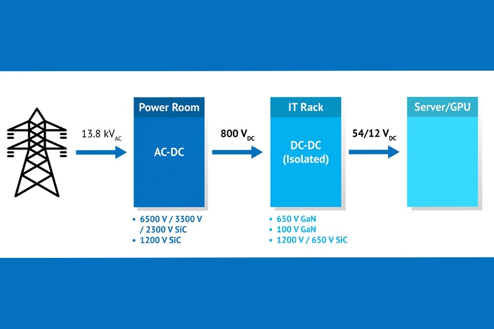
These rise of these two technologies has widespread consequences, including devouring huge amounts of electricity. Consumption is so high that many AI tech companies, such as Google, Amazon, Microsoft and Meta, are interested in nuclear power plants; and those producing EVs have already played a major role in driving up the proportion of global energy consumption associated with transportation to 30 percent, a figure only expected to increase.
To control the distribution of electricity, designers of AI infrastructure, EVs, and the likes of chargers and power supplies, have tended to draw on well-established silicon technology, which includes silicon IGBTs and MOSFETs. However, the performance of these incumbents is held back by the small bandgap of silicon. Due to this limitation, there is now a growth in sales of power devices with a wider bandgap, including those made from SiC and GaN.
Figure 1. An illustration of the growth setup and gas-flow channels for HF-VPE. For more details see D. Nakamura et al. “Halogen-free vapor phase epitaxy for high-rate growth of GaN bulk crystals” Appl. Phys. Express. 10 045504 (2017).
The strengths of GaN are not just a high breakdown voltage that results from the wide bandgap. In addition, GaN devices benefit from a high mobility. Thanks to these attributes, figures-of-merit for GaN are approximately 1,000 times higher than those for silicon, and exceed those for SiC by a factor of two to four.
A number of architectures are used to produce GaN devices. The lateral forms have enjoyed the greatest commercial success so far, but vertical power devices offer much promise – they are compelling candidates for serving in EVs/HEVs/HVs, where they combine a breakdown voltage of 1200 V with a current density of hundreds of amps-per-square-centimetre. If vertical GaN power devices were deployed in an electric vehicle’s power control unit, this would: drastically reduce its size, due to smaller inductive parts; and increase efficiency – and driving range – thanks to GaN’s excellent intrinsic material properties.
Barriers to GaN power devices
There are two big issues relating to material preparation – that is, growth – that must be overcome to realise feasible low-cost GaN power devices. One is the development of a cost-effective GaN bulk growth method. To ensure the manufacture of high-performance highly reliable GaN-based power devices there is a need to produce large, high-quality native GaN single-crystal wafers at low cost; therefore, it is essential to develop crystal growth techniques for obtaining bulk GaN crystals.
The other major issue relating to material preparation is to find a way to ensure high-purity and precise control of the dopant concentration in thick drift layers. In vertical power devices, unlike their RF counterparts, energy loss is governed by the resistive component of the n-type drift layer, employed to ensures a high blocking voltage. Due to this, there’s a need to explore a cost-effective, highly precise GaN epitaxial growth method for drift layers.
One of the difficulties associated with GaN is that it’s not possible to produce crystals with the established Czochralski growth method. This approach, employed to pull a silicon crystal from molten silicon, is unavailable, because the equilibrium N2 pressure of GaN is expected to exceed 6 GPa.
Figure 2. (a) Plan-view and (b) cross-sectional scanning electron
microscopy images of a thick HF-VPE-GaN layer (about 55 µm). The inset
photograph shows the visual appearance of the as-grown halogen-free
(HF)-VPE-GaN growth front (cracks originating from thermal stress due to
the thermal expansion difference between GaN and underlying sapphire
layers during after-growth cooling). Bright-field cross-sectional
scanning tunnelling electron microscopy images taken from a thin
HF-VPE-GaN layer (about 5 µm-thick) including the interface between
MOCVD-GaN and HF-VPE-GaN layers at g vectors of (a) 0002 and (b) 11<bar>20,
where mixed/edge dislocations are marked with/without green triangles.
For more details see D. Nakamura et al. “Halogen-free vapor phase epitaxy for high-rate growth of GaN bulk crystals” Appl. Phys. Express. 10 045504 (2017).
Due to this limitation, much effort has been devoted to developing alternative methods for producing GaN crystals, such as high-pressure nitrogen source growth, ammonothermal growth, acid ammonothermal growth, sodium-flux growth, and hydride vapor phase epitaxy (HVPE). Of these five, the first three are only appropriate for preparing the GaN seed crystals. Their low growth rates – less than 10 µm hr-1 – are insufficient for producing boules. For the production of commercially available freestanding GaN substrates, material is grown by HVPE, which can employ growth rates of more than 100 µm hr-1, and is capable of depositing GaN layers as thick a 1 mm on seed GaN substrates. Thanks to these strengths, freestanding wafers are produced by growing thick layers, prior to
substrate removal. However, during the growth of GaN by HVPE, the reaction of gaseous GaCl with ammonia produces an unwanted by-product, NH4Cl. This by-product, in the form of ash, increases maintenance costs and hampers the length of growth campaigns.
Figure 3. (a) Photograph of as-manufactured evaporator (Eva_#2) made of
TaC ceramic. (b) Schematic drawing of HF-VPE setup with an evaporator.
(c) Photograph of postgrowth evaporator completely wetted with molten
gallium. (d) Comparison of GaN growth rate and gallium feed rate with
and without gallium evaporators. For more details see D. Nakamura et al.
“Significant increase in GaN growth rate by halogen-free vapor phase
epitaxy with porosity-controlled evaporator” Appl. Phys. Express. 10
095503 (2017).
Eradicating halogen
To avoid this unwanted ash, our team from Toyota Central R&D Laboratory is pioneering the development of halogen-free (HF) VPE. This involves a switching of the source material from ammonia and gaseous GaCl to gallium and ammonia. Thanks to this move to halogen-free sources, our reaction produces GaN and hydrogen (see Figure 1). Our new process uses gallium vapour as the gallium source, with low pressures of around just 2 kPa enhancing gallium vapour supply.
Using this novel approach, we have demonstrated high-quality growth of GaN (see Figure 2). In addition, we have found that a porosity-controlled evaporator can enhance the molten gallium surface area, resulting in substantial increases in the gallium vapor supply and the growth rate, which can be as high as 700 µm hr-1 (see Figure 3).
Another benefit of HF-VPE is that it leads to a higher yield. With conventional HVPE, gallium material yield is around just 10 percent. In comparison, with our growth technology, yield approaches 50 percent, thanks to a simple reaction that’s free from any back reactions. This hike in yield, alongside the fast growth rate and the absence of unwanted by-products, underscores the capability of HF-VPE to deliver cost-effective growth of GaN bulk boules.
Our critical next step in the development of HF-VPE is the demonstration of thick GaN growth – that is, layers more than 5 mm-thick. To succeed, we need to address the parasitic growth of polycrystalline GaN around the seed crystal. This issue prevents lengthy growth, a pre-requisite for the production of high-quality bulk HF-VPE GaN.
We are investigating potential solutions to this issue. One is to introduce anti-parasitic reaction coatings, made from tungsten carbide, for our reactor components. Initial results are promising, with modified susceptors and crucibles ensuring a decrease in polycrystalline GaN formation around the crucibles (see Figures 5 and 6). Another idea we are pursuing, involving the use of crystal growth computer simulations, is to design a more appropriate ammonia nozzle that decreases formation of polycrystalline GaN around the GaN growth area.
Figure 4. Dependence of material yield of gallium during HF-VPE GaN
growth on seed substrate diameter. Insets show images of respective
as-grown samples and their surface morphologies. Hexagonal hillock
structures on the surface are due to direct growth on sapphire without a
buffer layer, and the blackish appearance of grown layers is due to the
optical confinement effect caused by hexagonal hillock structures. For
more details see D. Nakamura et al. “Ultrahigh-yield growth of GaN via halogen-free vapor-phase epitaxy” Appl. Phys. Express. 11 065502 (2018).
Improving the drift layer
By far the most common method employed for the growth of GaN epiwafers is MOCVD. This epitaxial technology, offering excellent controllability in terms of thickness and impurity doping concentrations, is used for commercial production of GaN HEMTs, as well as lasers and LEDs.
As previously mentioned, the resistive component of the n-type drift layer in vertical GaN power devices has a large impact on energy loss. This key layer is typically around 10 mm-thick, and requires a precise control of the net carrier concentration, in the range 1015 - 1016 cm-3.
According to the work of several researchers, carbon impurities that act as deep acceptor dopants can wreak havoc on vertical GaN power devices. The primary downside is a slashing of electron mobility that leads to mobility collapse, and in turn an extreme increase in on-resistance. Due to this, the drift layer must be grown with an impurity-free growth method. And while MOCVD is an option for this task, it suffers from several weaknesses.
The biggest drawbacks of using MOCVD for the growth of drift layers for power devices are a slow growth rate – it’s typically just a few microns per hour – and high levels of carbon impurities. Addressing the latter is far from trivial, as the source of gallium is a metal-organic. Due to these issues, it is impractical to grow the drift layer of a GaN vertical power device by MOCVD.
One alternative for the growth of a thick GaN drift layer, proposed by the Sumitomo chemical group, is to use high-purity HVPE. This approach, also known as quartz-free HVPE GaN, involves a reduction in the source zone temperature. To realise this, opaque quartz is introduced into the reactor. The refinement reduces radiative heat transmission and prevents heating of stainless steel used in the growth apparatus.
Sumitomo’s approach has delivered some success, with researchers from the company demonstrating GaN with a high-purity – levels of carbon are below 1 x 1014 cm-3. However, the halogen gas utilised for HVPE can increase maintenance costs, due to by-products. There’s the threat of a shortening of the growth apparatus lifetime, due to corrosiveness of the gas. What’s more, it can be challenging to precisely control the doping level in thick layers. This issue arises because the HVPE growth condition is generally close to atmospheric pressure, making it difficult to form the sharp turn-on/off of the silicon dopant along the depth profile, due to the dopant gas’s low flow speed. Furthermore, according to a team at the Institute of High Pressure Physics Polish Academy of Sciences, there are other difficulties in controlling the doping level with HVPE, due to unintentional silicon deposition inside the reactor or/and in the dichlorosilane line, used for silicon doping.
A better option for the growth of the drift layer is HF-VPE. This epitaxial technology offers high purity, thanks to the absence of carbon, and growth rates can be as high as a few tens of microns per hour. Another advantage of HF-VPE is that it’s easy to use any solid source material for the dopant source.
Our efforts on this front have involved silicon doping of GaN with a solid silicon source (see Figure 7). However, our initial results for electron mobility were lower than those for samples grown by HVPE, implying the possibility of large concentrations of other impurities. This finding questioned the promise of using HF-VPE for the growth of the drift layer in vertical-type power devices.
Figure 5. Plausible mechanism of the anti-parasitic reaction effect of
the WC catalytic layer based on surface nitride formation (accompanied
by H2, atomic H desorption, or both), which results in the absence of active nitrogen adsorbates (such as –NH, –NH2, and –NH3) for GaN formation. Surface nitrogen atoms desorb via N2 formation, which can cause desorption of gallium adsorbates. For more details see D. Nakamura et al.
“Tungsten carbide layers deposited on graphite substrates via a wet
powder process as antiparasitic-reaction coatings for reactor components
in GaN growth” Cryst. Eng. Comm. 22 2632 (2020).
We did not give up, with further efforts identifying the source of contamination in our GaN layers grown by HF-VPE: nitrile gloves used for growth preparation. These gloves are made from nitrile rubbers that contain silicates (for example, Mg3Si4O10 and calcite (CaCO3)), used as fillers. During furnace maintenance, eluted contamination from nitrile gloves attaches to growth furnace parts, before entering epilayers during growth.
Figure 6. Photographs of 4-inch seed substrate holders made of (a)
single-layer anti-parasitic-reaction-coated, (b) double-layer
anti-parasitic-reaction-coated, and (c) conventional pBN-coated (for
reference) graphite taken after HVPE GaN growth under identical growth
conditions (seed temperature around 1080 °C; V/III ratio around 20).
Gallium crucible outlets made of (d) double-layer
anti-parasitic-reaction-coated and (e) TaC-coated (for reference)
graphite after HF-VPE GaN growth under identical growth conditions (seed
temperature around 1250 °C; partial NH3 pressure 0.53 kPa;
growth time of around 0.5 h). Inset photographs were taken before growth
experiments. For more details see D. Nakamura et al. “Tungsten
carbide layers deposited on graphite substrates via a wet powder process
as antiparasitic-reaction coatings for reactor components in GaN
growth” Cryst. Eng. Comm. 22 2632 (2020).
After identifying the source of contamination and eradicating it, we have demonstrated that HF-VPE can produce GaN layers similar to those produced by our revolutionary ‘quartz-free’ HVPE technology, in terms of growth quality and dislocation density. According to secondary ion mass spectrometry, our HF-VPE grown GaN layer has carbon and oxygen concentrations no more than 5 x 1013 cm-3 and 1 x 1014 cm-3, respectively. This form of spectrometry could not detect any boron, iron, magnesium, aluminium, calcium, chromium, zinc, nickel, manganese, or manganese in our GaN epilayer (see Figure 8).
Figure 7. Relationship between the silicon concentration and net donor
(Nd-Na) concentrations of silicon-doped-GaN grown by HF-VPE. For more
details see T. Kimura et al. “Growth of high-quality GaN by halogen-free
vapor phase epitaxy” Appl. Phys. Express. 13 085509 (2020).
We have also investigated carrier transport characteristics. Following the elimination of unintentional impurities, our HF-VPE grown GaN exhibits a high electron mobility (see Figure 9).
Based on characterisation of our material, we can conclude that our HF-VPE growth method is capable of growing high-purity GaN layers with a low dislocation density. Thess layers can be thick, thanks to a prolonged growth time, and are produced with a high material yield. In addition, our study provides the first experimental evidence of calcium impurities, in addition to carbon and iron, functioning as deep acceptors. We verified that it is critical to avoid these calcium impurities, as they lead to mobility collapse in lightly doped n-type layers.
Figure 8. Depth profiles of impurity concentrations in the HF-VPE GaN layer after upgrading the process. For more details see T. Kimura et al. “Impurity reduction in lightly doped n-type gallium nitride layer grown via halogen-free vapor-phase epitaxy” Appl. Phys. Lett. 124 052104 (2024).
Our plans for the future include investigating whether HF-VPE with a magnesium vapour supply is able to produce p-type GaN layers with enhanced control and simplicity. Success on this front would give this approach the edge over the existing HVPE method, which uses a solid MgO source. Another promise of HF-VPE is better control over doped epilayers, due to the very-low-pressure growth environment of just 1- 10 kPa.
Figure 9. Dependence of Hall mobility (mH) on carrier concentration for GaN layers at 300 K. For more details see [1] Fujikura et al. Appl. Phys. Lett. 117 012103 (2020). [2] S. Kaneki et al. Appl. Phys. Lett. 124 012105 (2024). [3] N. Sawada et al. Appl. Phys. Express. 11 041001 (2008). [4] Y. Ohshima et al. Jpn. J. Appl. Phys. 45 7685 (2006). [5] S. Nakamura et al. Jpn. J. Appl. Phys. 30 L1705 (1991). [6] S. Nakamura et al Jpn. J. Appl. Phys. 31 2883 (1992).
There’s no doubt that HF-VPE has great potential to provide epitaxial growth for tomorrow’s GaN power device applications. A key stepping stone towards this goal is our demonstration of GaN layers that are devoid of carbon, iron and calcium impurities. Consequently, we believe that the HF-VPE growth method is a promising, cost-effective one for both bulk GaN and epitaxial GaN layers.


