Japanese team makes GaN-HEMT on 2-Inch diamond substrate
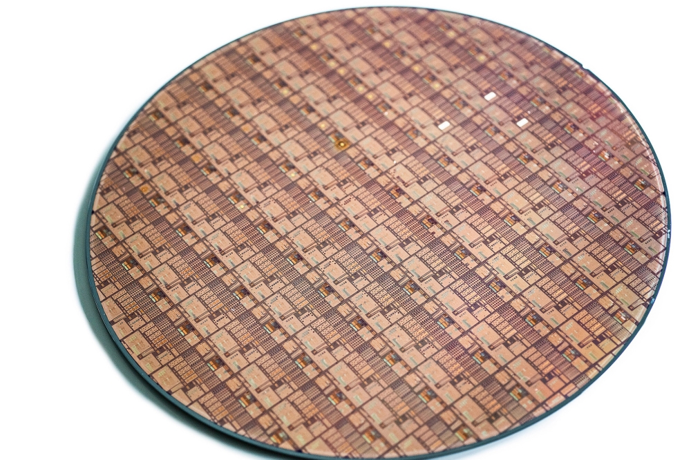
Sumitomo Electric and Osaka Metropolitan University have successfully fabricated a GaN-HEMT on a 2-inch polycrystalline diamond (PCD) substrate in a joint research project with the Japan Science and Technology Agency (JST).
They say that this technology is an important step toward achieving higher capacity and lower power consumption of core devices in mobile and satellite communications.
In recent years, as the volume of information in wireless communications has increased, there has been a demand for higher frequencies and higher output powers in devices such as GaN-HEMTs. However, the self-heating that occurs during operation limits the devices’ output power, resulting in signal transmission failures and other problems that reduce the performance and reliability of communications.
To address these issues, OMU has successfully improved heat dissipation characteristics by using diamond, which has extremely high thermal conductivity, as a substrate for GaN-HEMTs.
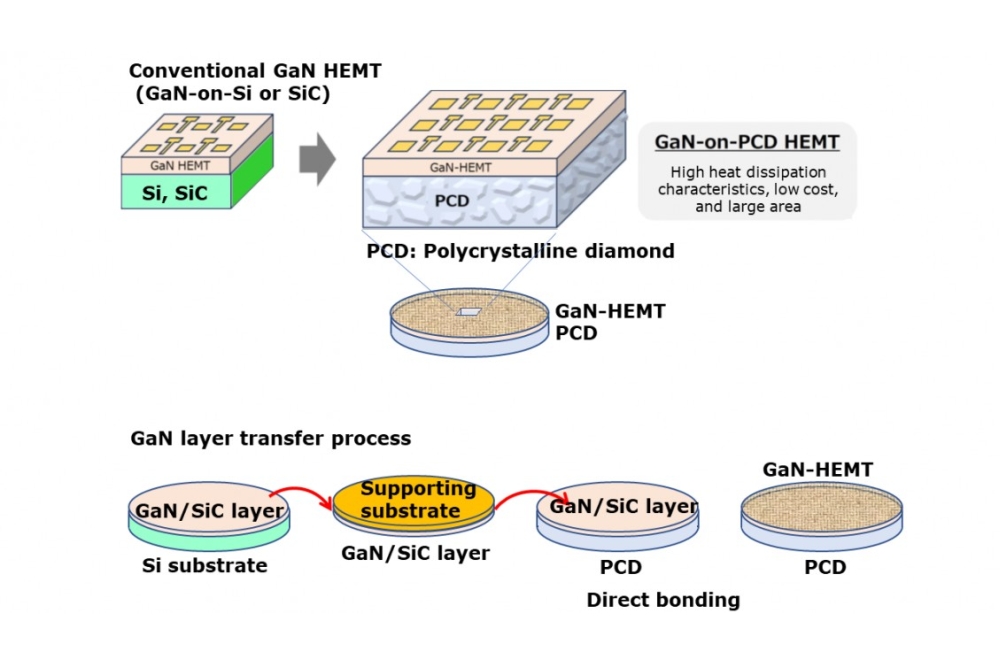
Generally, silicon and SiC are used as substrates for GaN-HEMTs, but the thermal conductivity of diamond is about 12 times higher than that of silicon and 4 to 6 times higher than that of SiC, so using diamond as a substrate can reduce thermal resistance by a quarter and half, respectively.
Previously, direct bonding to GaN layers without solder or bonding material was difficult due to the large grain size and poor surface roughness (5–6 nm) of polycrystalline diamond. However, Sumitomo has managed to directly bond a GaN layer to a 2-inch polycrystalline diamond substrate using two approaches. First by diamond substrate polishing technology to reduce the surface roughness to half the conventional level and second by integrating OMU’s technology to transfer the GaN layer from the silicon substrate onto the polycrystalline diamond.
As a result, the team has demonstrated the GaN structure on polycrystalline diamond and its uniform heat dissipation characteristics. The GaN layer used in this study was provided by Air Water . as a GaN/SiC epitaxial layer on a silicon substrate.
Future developments will be to improve device performance and optimise bonding conditions using 4-inch substrates aimed at mass production.