Soitec and PSMC announce 3D stacking collaboration
France-based semiconductor materials company Soitec has announced a collaboration with Powerchip Semiconductor Manufacturing Corporation (PSMC), a Taiwan-based memory and logic foundry.
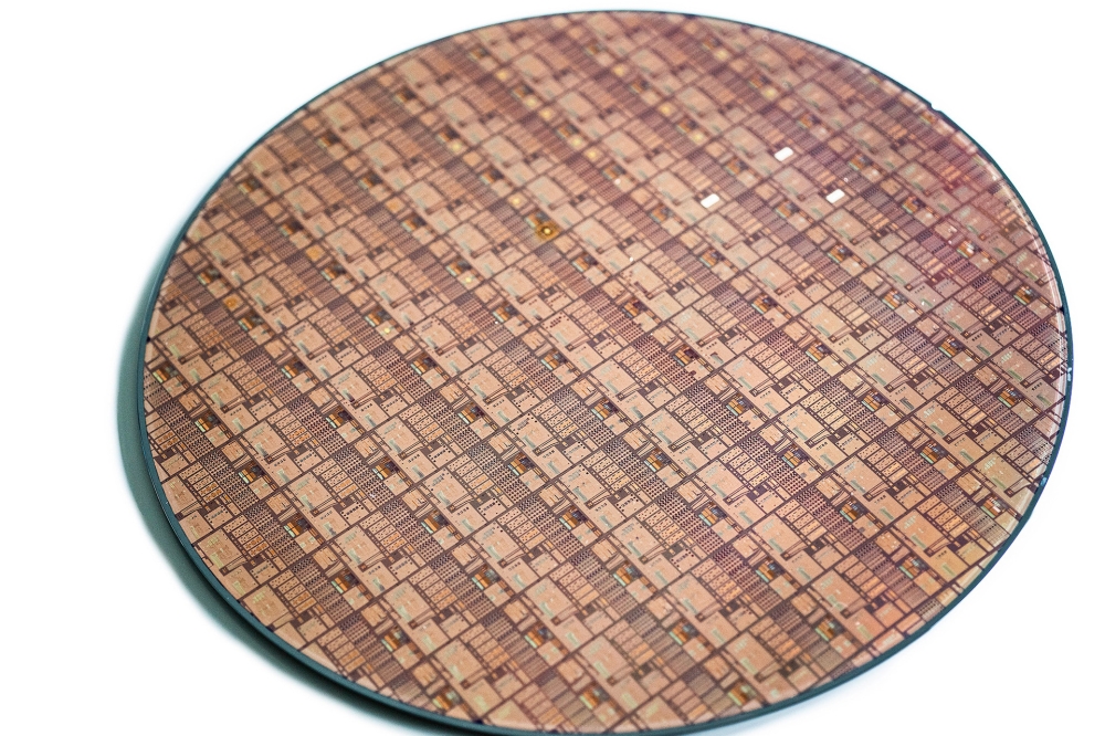
Under the collaboration, Soitec will supply PSMC 300mm substrates incorporating a release layer, Transistor Layer Transfer (TLT) ready, to support a new demonstration of advanced 3D chip stacking at the wafer level. This marks the first public announcement of Soitec’s TLT technology.
This new substrate stacking approach is designed to enable high-speed transfer of ultra-thin transistor layers onto different types of wafers — a key requirement in heterogeneous integration.
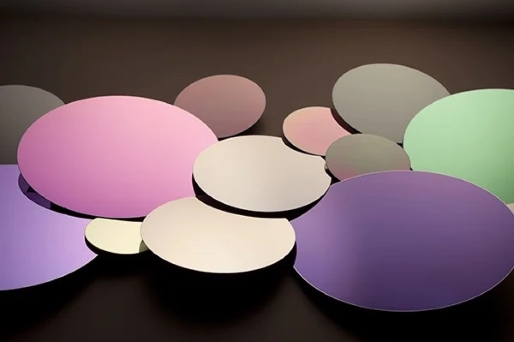
The approach is based around Soitec's Smart Cut technology in which a thin crystalline material layer 5nm to 1µm in thickness can be transferred from a piezoelectric donor substrate, SiC, GaN, InGaN or InP to another substrate.
Soitec describes Smart Cut as working like a "scalpel on the atomic scale" making it possible to position a crystalline layer on all types of materials, and generate active layers of structures independently of the mechanical support substrate.
Once devices are fabricated on the TLT wafer, an IR laser process facilitates the lift-off of the ultra-thin layer from the substrate to the target wafer.
The technology is said to be an enabler for a wide variety of next-generation semiconductor designs with potential applications ranging from smartphones, tablets and AI devices to autonomous driving systems.
Soitec’s CTO and senior EVP Innovation, Christophe Maleville said: “ Our collaboration with PSMC reflects a shared commitment to pushing the boundaries of 3D integration and supporting the global shift toward more efficient and compact computing architectures. Together we are laying the groundwork for the next generation of semiconductor innovation.”
PSMC CTO SZ Chang said: “In the two-year collaboration, PSMC has demonstrated an innovative wafer-stack integrated process by leveraging Soitec's advanced substrate technology. The innovation significantly broadens the 3D technology from chip-level stacking - optimising power performance in computing architecture, to transistor-level stacking – extending Moore’s law, with a remarkable reduction in stacking wafer thickness from micrometer to nanometer level.”